Main Menu
Serial Input Paralel Output Sipo
суббота 02 марта admin 38
Oct 25, 2018 - To convert between serial-parallel – Since we have both serial and parallel types of inputs and outputs, we can use shift registers to convert.
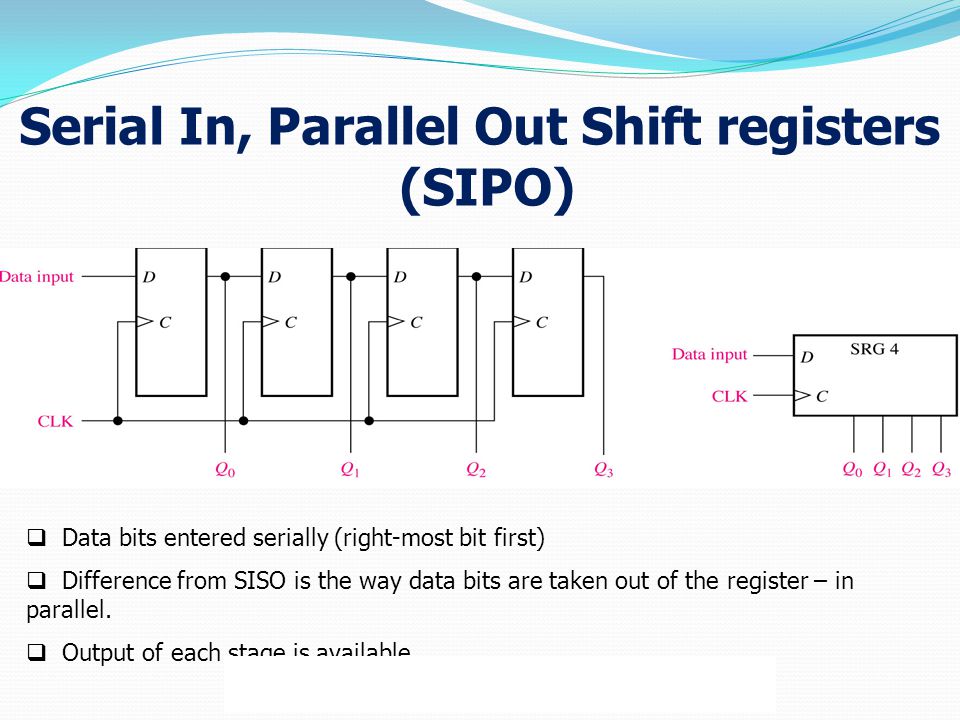
The operation of SIPO is as follows. Lets assume that all the flip-flops ( FFA to FFD ) have just been RESET ( CLEAR input ) and that all the outputs QA to QD are at logic level “0” ie, no parallel data output. If a logic “1” is connected to the DATA input pin of FFA then on the first clock pulse the output of FFA and therefore the resulting QA will be set HIGH to logic “1” with all the other outputs still remaining LOW at logic “0”. Assume now that the DATA input pin of FFA has returned LOW again to logic “0” giving us one data pulse or 0-1-0. The second clock pulse will change the output of FFA to logic “0” and the output of FFB and QB HIGH to logic “1” as its input D has the logic “1” level on it from QA. The logic “1” has now moved or been “shifted” one place along the register to the right as it is now at QA. When the third clock pulse arrives this logic “1” value moves to the output of FFC ( QC ) and so on until the arrival of the fifth clock pulse which sets all the outputs QA to QD back again to logic level “0” because the input to FFA has remained constant at logic level “0”.
The effect of each clock pulse is to shift the data contents of each stage one place to the right, and this is shown in the following table until the complete data value of 0-0-0-1 is stored in the register. This data value can now be read directly from the outputs of QA to QD. Then the data has been converted from a serial data input signal to a parallel data output. The truth table and following waveforms show the propagation of the logic “1” through the register from left to right as follows.
5.7.1 Parallel In/Parallel Out (PIPO) Register An electronic register is a form of memory that uses a series of flip-flops to store the individual bits of a, such as a byte (8 bits) of data. The length of the stored binary word depends on the number of flip-flops that make up the register. A simple 4-bit register is illustrated in Fig. 5.7.1 and consists of four, sharing a common input, providing synchronous operation ensuring all bits are stored at exactly the same time. The binary word to be stored is applied to the four D inputs and is remembered by the flip-flops at the rising edge of the next clock (CK) pulse.
The stored data can then be read from the Q outputs at any time, as long as power is maintained, or until a change of data on the D inputs is stored by a further clock pulse, which overwrites the previous data. Different types of register are generally classified by the method of storage and readout used; this basic form of register is therefore classified as a ‘Parallel In/Parallel Out’ (PIPO) register.
Shift Registers. Shift registers have a similar structure to the PIPO register but have the added ability to shift the stored binary word left or right, one bit at a time. Victoria hdd test windows 7 download full. This makes them extremely useful for many applications. They are used in handling serial data and converting it to parallel form or back again to serial form, and therefore are an essential component in communication systems. Shift registers are also essential in arithmetic circuits where binary numbers may be shifted right (and so divided by two), or left (multiplied by two) as part of a calculation. Shift registers can be used to delay the passage of data at a particular point in a circuit.